Friday, March 15, 2019

70 W eBay MOSFET HF Amplifier

I'd been working on my phasing receiver for about four years and decided it was time to team it with a TX section so I could make some QSOs and say "RIG HR IS HOMEBREW", a goal I'd had for some time. Not a QRP rig this time, but something in the 50 to 100 W range. I'd already taken a step in that direction by building a little Class E amplifier for 40 and 20 meters using three TO92 MOSFETs and supposed to produce 5 Watts out. (Lotsa luck on that ...) That could be my driver.

OK enough preliminaries. I read about the eBay amp on one of my ham mailing lists and I thought at the price, why not give it a shot?


I paid $18.57 ppd for it. It's said to be a class AB linear amplifier for SSB AM CW FM power amplifier for low-power radio power connection and suitable for FT-817 KX3 other small power stations.

It's basically a "bag-o-parts" and a circuit board. No schematic, no instructions. But you can find lots of stuff on the web, fortunately. Your fellow hams always helping out.


Here's what I got in the parcel from China. The board seems to have good quality. The parts look OK too - tubes for the one-turn transformer windings, ferrites, insulators for the TO220 parts, including shoulder washers.  And in my case, some SMT parts were pre-soldered. A nice bonus. The MOSFETs have had their part numbers removed. Ham community says IRF-530.

The board has some parts that you break out and use for the ends of the toroids, to solder the tubes that extend through the binocular balun holes to. This leaves two rectangular openings. The smaller ones are where the MOSFETs mount and bolt to the heat sink below. The larger one is where the big ferrite cores for the output transformer go. 

Finding some info ...

I found some very useful info on the web, including a YouTube video or two.

OE1CGS has some really good info, including a PDF he put together on the amplifier, some of which has been translated into English.

http://www.oe1cgs.at/50w-hf-verstaerker/

Finding a decent schematic can be difficult. You may find that some look good initially but lack sufficient resolution to read part numbers and values with confidence. I eventually did find a pretty good one.

Here's another good page on the amp, with measurements and good photos from DK9JC:

https://www.dk9jc.de/blog/equipment/142-diy-kits-70w-ssb-linear-hf-power-amplifier-ft-817-kx2-kx3

PD7MAA has more good info, Lowpass filter design info, a schematic and more good photos:

http://pa-11019.blogspot.com/2016/11/diy-kits-70w-ssb-linear-hf-power.html

Some discussion of the circuit ...

The circuit is fairly standard. It includes some frills like a regulator and pot to set the bias voltage / idling current. And a switch-around relay that feeds the antenna around the amp to the driver when 12 V is not applied, and through the amplifier when it is. There is a 2-pin header labeled PTT that when closed turns on a small PNP transistor which feeds the bias regulator and also feeds 12 V to the relay. The MOSFET drains are always connected to the 12 V line. I keep a shorting jumper across the PTT pins.

The MOSFETs have 150 ohm feedback resistors from drain to gate through blocking capacitors. Except mine were not 150 ohms as shown on the schematic. Was this a design decision, or did they just run out of 150 ohm resistors?  Who knows? Mine are 100 Ω. 

One thing that seemed to be something of a glaring omission was the lack of any kind of swamping resistors on the input to set a constant resistive load to the driver. I initially used my KX3 with ATU to try to get a good match but after reading comments and suggested resistor values from OE1CGS, I added the resistor (21 Ω). It's across the secondary of the input transformer. After that, my driver was looking at a much better SWR.

Some notes on building & testing ...

My building notes are exhaustive (tedious?) so I'll try to hit the high points. Of course, fit up the pieces and understand how they go together before soldering anything. The photos on various blogs I found to be helpful for that purpose. I copied some down to my own folder.

One thing to be careful of - the tabs of the two MOSFETs are head-to-head and there needs to be a gap between them or there will be a short. Keep that in mind. Maybe stick a little insulating shim like a piece of toothpick between them before soldering. 

And of course, the board is designed to sit on top of the heat sink and the MOSFETs bolt directly to it, with insulators. It's important to have full contact area and tight hardware. I think a few folks thought they'd test very briefly with no heat sink and blew their MOSFETs.

Since my board came with the voltage regulator components pre-mounted, I hooked up 12 V before putting anything else on the board and verified that it was working and that I could vary the voltage with the little pot.

After mounting all the parts, I wanted to set the bias. Even with no drive, I felt that I needed to hook up a load to the output in case of self-oscillation. Or maybe to prevent it. And 50 Ω across the input isn't a bad idea either. Another good safety practice might be a switch or hand key across the PTT pins in case the circuit runs away and you want to shut the bias off quickly.

The schematic shows 2.7 V bias. Most people find that too low. Adjusting it until the MOSFETs are carrying a little drain current is a good idea.

I tried various values of idling current, up to 120 mA or so, but eventually set on about 30 mA total current. The relay coil draws about 42 mA at 12 VDC, so subtract that off of the total reading from the supply. Or adjust bias to minimum, note the current, then increase until current increases by 30 mA. My bias voltage was 3.41 VDC at 30 mA total MOSFET current. Setting current higher might be OK but think about dissipation. 

For full power testing, a good dummy load is a good idea, since there's no SWR protection here. A way to monitor power - RF probe, power/SWR meter or oscilloscope is desirable.

A way to control the drive power is good too as gain varies on different bands. Maybe a 1 W output TX could be a good starting point. I think testing without an LPF into a dummy load is fine. Jumper across the LPF - using the supplied 0.1" pin headers.

I would not recommend going key down for longer than a few seconds, maybe 5 maximum until you know where you stand. I have a cheap Harbor Freight IR thermometer that I'd point at the transistor bodies and get a relative idea of how much they warmed up from a few seconds key down, and then to be sure they'd cooled down before doing another key down session. Feeling the heat sink is not a good way to see how things are going, in my opinion.


Some deviations in what was supplied and other info ...
  • MOSFET numbers are sanded off. Unknown P/N. I ordered 10 IRF530N from eBay.
  • Feedback power resistors are 100 Ω, not 150 Ω.
  • R1, R2 and R3 are 3900 Ω, not 10 kΩ.
  • R7 is 200 Ω, not 1 kΩ.
  • Pot VR1 (or VR3) not marked but measured and calculated as 785 Ω. Possibly a nominal 1 kΩ.
  • Some bloggers said adjust bias to 3.7 VDC, not 2.7 VDC. I used 3.41 VDC. It probably varies. With 3.7 VDC, my drain current "took off".

Results ...


With 1 W input:

BAND
SWR
WATTS
80
1.2
61.1
40
1.5
45
30
1.4
25.3
20
1.4
16.2


Of course I can get more power by increasing the drive on the higher bands. This is without a LPF, but I noted on 40 meters that power didn't decrease noticeably when I added the LPF.

On the air ...

So far I've just used it on 40. My Class E transmitter puts out too much power on 40 (4.2 W) and not enough (2.3 W) on 20!  So I built an attenuator for 40 meters to give 1.2 W drive. With that and a 13.0 VDC supply, I'm putting out a hair over 50 W. I'm a bit afraid to try for 70 W until I get more experience with it.

I lashed everything together with my homebrew phasing receiver, keyer and T/R switch and started making contacts. It's a lot of fun, as I expected. I've had some fairly long QSOs and some strings of contest QSOs with no performance issues. I put an antenna tuner in line and make sure the SWR is as flat as possible before transmitting.

BTW, the driver for the Class E section is my Si570 synthesizer, which also is used with the receiver. I had to add to the software to have it do the CW offset shift on key-down. I'll need other features (RIT, for example) shortly. But I'm getting off-topic ...

MOSFET failures ...

Everyone has them. I've had them twice. Once was cause by "human error" - I created a short with the lash-up of parallel resistors used for my 21 Ω swamping resistor. The second time it was simple over-heating, I think. Key-down too long and/or mounting hardware for the TO220 tabs not tight enough.


Here's a photo of it mounted on its over-sized heat sink, with LPF on the left and input attenuator below. The blue resistors are the feedback resistors. The gray ones in parallel with a smaller blue form the 21 Ω added swamping resistor. I hope to replace that with one properly sized resistor eventually.


Here's the schematic I downloaded from the PD7MAA site. It may not be hi-rez enough to build by as shown here, but I just want to give an overall view of the thing.

Some more about heat sinking and thermal issues ...

A large heat sink is a plus, but no matter how big yours is, a lot of heat has to flow through a small contact area to keep the MOSFETs from failing. Solid contact, good thermal conductivity through the insulator and adequate bolting force are necessary.

I was reading part 2 of WA2EBY’s popular MOSFET amplifier article in QST of April 1999. He noted that even with proper heat sinking techniques, his amplifier might exceed the maximum allowable temperature for the MOSFETs if it were held key-down for more than five seconds. However, he was able to send a string of continuous dits without overheating. So it's on the edge and if the duty cycle is kept withing typical ham CW/SSB values it will do OK.  I hope.

Final thoughts ...

Well, for my eighteen dollars and change, I think I got a decent little project and learning experience. I need to do more with it of course, and integrate it better into this theoretical transceiver I'm constructing.

Is it homebrew?  We worry about such things. Well - it's a nice board and bag of parts, but you get to find a schematic, fix a design flaw or two, build one or more LPFs, decide how to drive it, blow up some MOSFETs and learn from the experience.  So I guess it might qualify.


Tuesday, November 14, 2017

PIC Frequency Counter With Morse Output

It's a little strange to blog about a project that's mostly software, but even if I don't explore the software design in depth I can at least describe the resulting instrument.
For hams who program MCUs, a frequency counter seems to be one of several obligatory projects, with others being a keyer and a controller for a DDS or PLL type synthesizer. So I wanted to get in my frequency counter project.
Counters such as this one have been around for a while, often integrated into radios with analog VFOs. With the tap of a button, you hear the frequency accurately announced in Morse and thus the need for a calibrated dial is avoided.
I said "With Morse Output" but it's common to refer to the device function as AFA, for Audible Frequency Annunciation.
Before I ramble much more, let me list the features of my counter. Every programmer likes to add a wrinkle or two to previous implementations and I've added one or two:


Features
One button control to initiate count or menu actions
User programming of superhet IF frequency offset
Selectable 1 Hz or 100 Hz resolution
Option to suppress higher digits for faster readings
Can be built SMT or through hole
Small size - I used a RS proto board 1.75 x 2.75 inch
Setup saved on EEPROM and recalled on power-up
Three selectable Morse annunciation speeds
Selectable audible marker for each 1 kHz change while tuning

Specifications (approximate)
Accuracy:  Depending on the time base, can be as good as 1 Hz
Resolution: Selectable to 1 Hz or 100 Hz
Response time: 1 s for 1 Hz resolution and 10 ms for 100 Hz
Sensitivity: 35 mVpp to 180 mV through 6 meters
Idling current draw at 12 V input is 11 mA
My prototype SMT version will read to just over 140 MHz
Minimum frequency is about 50 kHz with input capacitor shown

Some hardware notes and schematic
I'd switched from PICs to AVR MCUs a few years ago but the PIC is unique in having a prescaler that can count really fast - independent of the chip's clock. So I went back to the 16F683 8-pin PIC for this project.
I looked at several other designs although I didn't have their source code to guide me. Some use Microchip's AN592 app note as a starting point, but its accuracy can degrade to 1 kHz or worse at higher frequencies. I liked the Stinger Singer counter sold by the Arizona SQRPions group and designed by Dan Tayloe. The use of a 74HC00 AND-gate package allowed precise gating of the input stream and also gating out and counting the remainder stuck in the prescaler, which can't be read directly.


Sorry it's fuzzy. I'll provide a link to a better schematic.

I built my DIP version on a Radio Shack 276-150 prototype board. Radio Shack is gone but I found some at B.G Micro. I also built a SMT version on a board I made using the toner transfer technique. You could omit the programming header if you have a pre-programmed chip.

Want to try it?
I've added a link to the HEX code. You can burn it to a PIC with a PICkit-2 or PICkit-3. Or I could program a PIC for you and mail it in the USA. Say $4 to buybye@suddenlink.net which is my PayPal address. Or four ones to my QRZ address. First make sure I'm still alive and capable of fulfilling the request by emailing me at kennnick@gmail.com.
I've also linked a manual below, with a lot more info on building and operating the counter.

Possible improvements
I like the feature I added to give an audible "tick" marker with every kHz of change. But it introduced an artifact. When this feature is ON, the counter must read the frequency continuously and the pin that drives the speaker is also used in counting logic. This results in a low "puttering" sound from the speaker that's almost but not quite inaudible. Of course you can turn it OFF if it's a bother. One fix I've considered is to use a separate crystal oscillator with a transistor for the timebase. That would free up one PIC pin to dedicate to the speaker. Another fix would be to use a higher pin count PIC. But a 14 or 18 pin PIC would make the counter so much larger. I could justify it by integrating a keyer function into the chip as others have done. That would make it worthwhile.

Files


73,
Nick, WA5BDU

Tuesday, March 7, 2017

PIN diode T/R switch

100 W T/R switch in box

I like to play with separate transmitters and receivers, either those I'm building or a few classic boat anchors I'm hanging on to.

Back in the 60s I participated in NTS (National Traffic System) nets where full QSK was part of your entry ticket if you wanted to be taken seriously. But even though I've grown used to the smooth "semi-break-in" of modern transceivers, the notion of "electronic T/R switching" has a mystique for me and I've always wanted to try it.

Description

First let me try a brief description of the switch if I'm capable of it (being brief), before I get into tedious detail over why I chose every minor component in the circuit.

The goal was for it to handle 100 watts on 80 through 10 meters and 6 if possible. Minimal SWR caused in the transmit path, less than 1.2 if possible. As much isolation as possible between the transmit and receive ports. I measured from 68 dB on 80 meters to 60 dB on 10 meters to 53 dB on 6 meters between the TX to the RX ports. That gives at most 0.1 mW to the receiver on 80 through 10. That's a loud signal but not destructive.

SWR to a 50 ohm dummy load is generally about 1.15, rising a bit a 3.5 MHz and 50 MHz.

The circuit uses back to back PIN diodes in the paths from antenna to transmitter and again from antenna to receiver. One pair is biased to conduct in PIN diode mode with forward current while the other is reverse biased with high voltage to the OFF or blocking condition. These biasing conditions are swapped to switch between transmit and receive.

The PIN diodes are actually common rectifier diodes which happen to have a PIN type structure. This is primarily in the interest of keeping costs low in the ham tradition.

Circuit


This is the main portion of the schematic, less the power supplies. The apparent complexity is reduced  when you see what's happening in the circuit.The two IRF830 MOSFETs control whether the diodes are in conduction mode or blocking. The '2222A inverter after the keying input causes the MOSFETs to be in opposite states, one on and one off. 

Consider the four current paths at the top from the 13.5 volt supply, when enabled these paths provide forward current of about 100 mA forward through each diode. Follow through the limiting resistor, two chokes, diode, then two more chokes and then the MOSFET to ground. One MOSFET will be ON and the other OFF, so either the TX or RX diodes will have forward bias current through them.

Next look at the 180 VDC supply coming from below and connecting to the drain of each MOSFET via 100 k resistors. For the MOSFET that is ON, that voltage is simply pulled to ground. But for the one that is OFF, the voltage appears between the cathodes of the diode pair, keeping them well reverse biased.

Besides antenna to TX and antenna to RS, there's one other somewhat optional path to consider, which is via the 1N4007 diode pointing down just left of the RX connector. This is a shunt path connection to provide an additional path to ground for any RF that makes it through the back-biased 1N4007s in transmit mode. In receive mode it is reverse biased with the high voltage supply and doesn't conduct.


Component choices


First, why two chokes in series at each location?  I copied from the design of WB9JPS (NA6O) on this. I'm not sure why he did it, but I have a fear of unknown self-resonance frequencies (SRF) in molded chokes when I'm trying to cover such a broad frequency range. I suspect the toroids with only ten turns will be fairly free of resonance which would address this concern. Probably just the toroids alone without the molded chokes would have been OK.

Next, the transmit path capacitors. For RF, ceramic capacitors such as type NP0 and dipped mica capacitors are usually specified. Capacitors described loosely as "film" types are said to have excellent characteristics for audio, but how do they do at HF and low VHF? Are they inductive?

So I got a little carried away with testing. My test consisted of putting the capacitor in series with the coax from my 100 W transmitter going to a dummy load. I checked SWR on 80 through 10 meters (and usually 6 as well). I held key down for 15 seconds and looked at temperature rise of the capacitor with my cheap IR temperature detector. Before hitting them with 100 W, I looked at SWR in a broad scan using my VIA (a sort of antenna analyzer).

I won't report all of the results here except to say that everything I tested did mostly "OK" - no huge SWRs or serious heating (one degree or so typical). I checked some large rectangular ceramic "disks", orange 400 V PETP 0.01 uF (three in parallel) film capacitors, large white 0.68 uF rectangular film capacitors also 400 V and four 0.01 uF SMT 500 VDC capacitors in parallel.

So I chose the big ceramics as  looking pretty robust and testing well. For other paths and bypassing I used SMT 0.1 uF, 500 V capacitors I have in my junkbox.

Now, the PIN diodes. Type 1N4007 are often used. Hayward used 1N4006s, which are also PIN diodes. For the transmit path, the 1N4006/4007 might be marginal for the 1.4 A rms required for 100 watts. Hayward and WB9JPS both used NTE5815. I think a 1N5408 is reasonably equivalent and I have them in my junk box. These are 3A diodes so I get some margin at the expense of greater capacitance. If I'd set my target at 50 W, the 1N4007s would have been OK in the transmit path. 

After these choices, there's not much that's critical.

Power supplies

My first idea was to use an external 12 to 14 VDC supply and provide the somewhat "high" voltage using one of those boost modules from eBay. But the little switcher was just too noisy, despite my efforts to filter it. In hindsight, I'm connecting it right to the receive antenna, more or less, so it would have to be super clean to be acceptable. So I went "linear" and power my switch from 120 VAC. 

For the HV, an obvious approach would be to use two back to back 120 to 12 VAC transformers to provide isolated 120 VAC and rectify that to 170 VDC. But I didn't have enough room so I stole a transformer from a Knight capacitor checker with magic eye to give about 130 VAC.  This one has to supply just about zero current so a simple capacitor filter following a bridge and it's done.

Oh, let me show the schematic before I continue:


Not much to explain in the low voltage section, but why the 78L12 regulator?  The unregulated 13.5 V output jumps to 25 V with no load. By design, the no load condition should never happen, but to protect the logic devices I have now and any I may add in the future I added the regulator. The 10 and 2.2 ohm resistors are my obsessive attempt to get to just the voltage I want for the bias current supplies. The low voltage supply uses a little plastic bridge while the HV uses four 1N4004 diodes. The 12.6 VAC transformer needs to be rated 400 mA or better.

Diode measurements and LTspice

My proposed diodes got a treatment similar to that I gave the capacitors. I wanted to be sure all this stuff really worked before committing to building. I made a jig to measure diode capacitance at 200 V reverse voltage and at or near 0 V with my AADE meter. 

1N4007:  2.1 pF @ 200V, 20.5 pF @ 0 V
1N5408:  9.2 pF @ 200 V, 76 pF @ 0 V

So the high voltage bias not only prevents the transmit waveform from forward biasing the diode but also keeps the series capacitance as low as possible.

I was trying to do a PIN diode T/R switch in LTspice using a downloaded 1N4007 model but the diode didn’t work like a PIN. I searched the LTspice Yahoo page and found a question by Don Huff W6JL with the same problem. He was told his model needed a Tt= statement in it for PIN behavior. I copied the text for his successful 1N4007 and now it shows PIN diode behavior.
Also, most models have Cjo specified at 0 V bias. So you don't see the lower Cjo you get with high reverse bias. I could change that to the value measured with high reverse bias, but of course it's only valid in that condition. But still to get a good prediction of performance it can be worth changing these values when switching between transmit and receive mode analysis.

PIN diode behavior and bias currents

RF switching with diodes can be done with "conventional" diodes, but the PIN diode is a different animal. Charge carriers that remain in the 'I' region of the diode allow current to flow in the reverse direction for a time after polarity switches to reverse during an RF waveform. So the diode is acting more like a low value resistor than a diode.

These charge carriers will be used up after a time, so there is a low frequency limit to this effect as well as a power (current) limit. This is why I'm not trying 160 meters. Note that the DC bias current serves to create the carriers, but its magnitude does not have to approach the maximum current of the RF waveform. I'm not certain how the required current magnitude would be calculated, but Hayward said, "I've found that a current of 100 to 200 mA is more than enough for 7-MHz operation at the 100-W level in a 50-ohm system." Note that at 100 W, peak RF current is 1.4 A.

Just as the PIN diode effects limit low frequency performance, the diode junction capacitance with reverse bias limits the amount of isolation obtained at the highest frequencies.

Board and enclosure

Recently I've been using the toner transfer method of board making for all but the simplest projects. I use SMT as much as possible since I don't like drilling holes. In this project I used a significant number of "leaded" components, but adapted them for surface mounting as can be seen in the photo.

The enclosure is a steel chassis I had on hand. I found that the two transformers generate a surprising amount of heat for their size and power ratings, so I'll probably drill some holes for ventilation when I put the cover plate on. 

Performance and enhancements

I made a number of measurements of isolation and SWR which looked good, but here I'm speaking of on the air performance. I used the T/R switch between my Knight T-60 transmitter and Drake 2B receiver during an on the air activity for several days on 40 (mostly) and also 80 and 15 meters. No failures or problems were experienced, just smooth T/R switching.

T/R switches such as this are often integrated into a "sequencing" system which keys various transmit stages, receiver muting, sidetone and so forth. I don't have much need for sequencing at the moment but might choose to design a keyer on a PIC or AVR chip so I can simply plug my paddle into the T/R box and have outputs to key the transmitter and/or VFO. A sidetone and muting are other options I might choose to incorporate.

Do it again, smaller

I allowed myself plenty of room for this project, which in the world of boatanchors is OK. But I think I could do a lot to make it smaller, especially if the target power level were 50 W or less. First, use a single choke in each bias leg, whether molded or toroid is found to be better. Then use more SMT devices, especially for the diodes and capacitors. And surely there's something smaller than IRF830s to handle 350 mA or so in saturation and block 200 V or more with margin.

The issue of generating the "high" voltage without RF noise will still require some thinking.

A problem and a fix

I was pretty pleased using the T/R switch with "novice" transmitters like the DX-60 and HT-40, with 30 to 45 watts out. But I got a surprise when I tried it with my HT-37, which puts out perhaps 100 W. 

On key down, the SWR zoomed. I eventually found that the T/R switch was switching between transmit and receive at a high rate - maybe 50,000 Hz or so. I tried many fixes and theories to no avail. At one point I found that a capacitor was "singing", but when I replaced it with a different type, it sang too. So it was responding to the problem, not causing it.

I found that I could start at low power and then run it up to 100 W with no issue, but keying at 100 W set off the oscillation.

I put it away a couple years and when I returned I started thinking about time constants. In NA6O's circuit, he used 0.022 uF capacitors from the drains of the MOSFETs to ground, and even sketched in the time constant. I didn't have that value in the voltage required in SMT so I substituted 0.1 uF. Realizing that this might be the problem, I changed those caps to two 0.01 uF units at each location and tried the switch with a 100 W transmitter. Success!

Potential builders please note: I have not changed my schematic as yet, so be aware of the change described above if you build a T/R switch based on mine.

Files

Schematics get a bit fuzzy and hard to read pasted into this blog. I'm going to put a schematic image and the ExpressSCH format file of the schematic into the Dropbox folder linked below. Also the ExpressPCB file for the board and anything else that seems useful.

References

"Electronic Antenna Switching" by Wes Hayward in QEX, May 1995. Also on EMRFD CD
"Experimental Transmitter" on the website of Gary Johnson WB9JPS (now NA6O):
http://www.wb9jps.com/Gary_Johnson/TR_Switch.html
QRZ.com page of Don Huff W6JL
Also see the Magic Box T/R switching system in 4SQRP.com, by K8IQY
I note that my schematic is very close to that of NA6O with component substitutions and power supply design variations noted.

Friday, September 2, 2016

Collins T-368 T-195 VFO to solid state


This started when I read a user's group post by Rick Campbell KK7B about these Collins VFOs that were at least at one time easily available from hamfests at low prices. And furthermore, they could be converted from tube operation to solid state without much difficulty. The advantages are low drift and low phase noise, among other things.
So I started looking around and found one at my local hamfest for $10. The total package is actually an exciter. The VFO covers 1.5 to 3.0 MHz and the chassis includes multipliers to give x2, x4, and x8 ranges. You can see why it needs to be stable if you're going to multiply by up to eight times.
I figured out how to energize just the oscillator section (two tubes) B+ and filaments and had some fun playing with it and measuring the drift. Then into the attic with it for several years, with conversion to solid state a back of the mind notion for "some day", which just arrived this week.
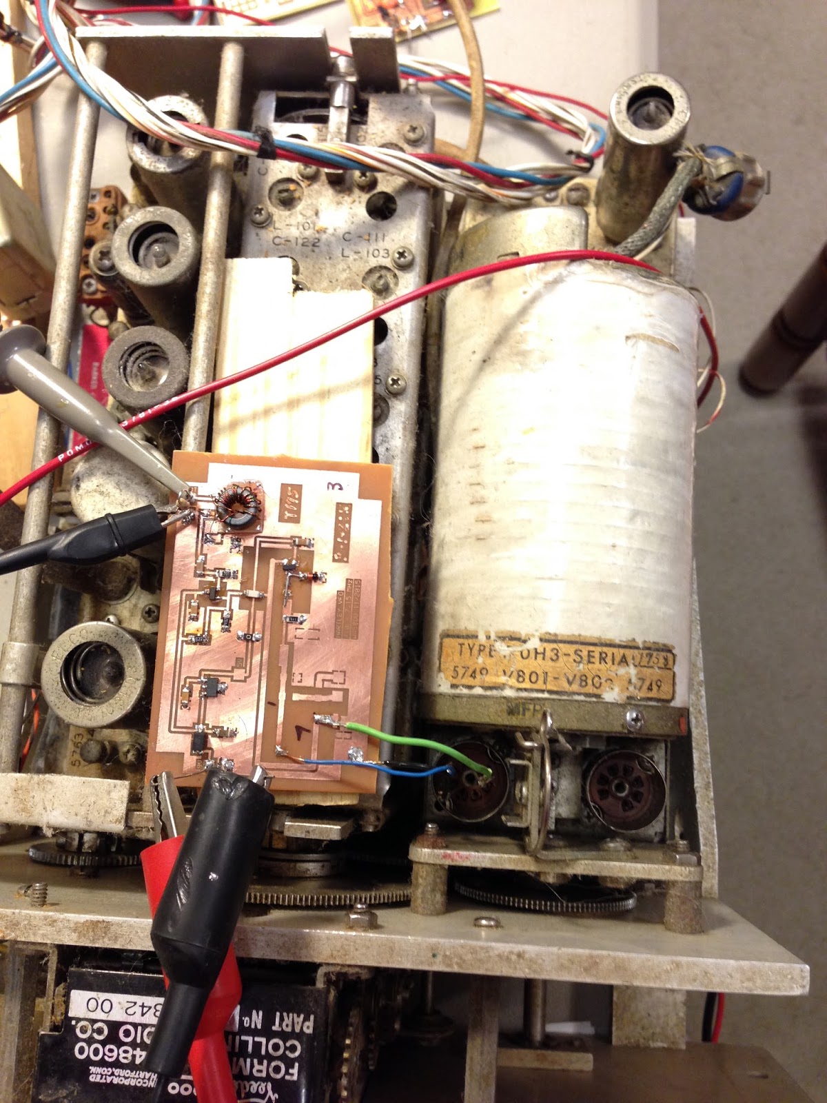
The magic is in that white soup can. It houses the frequency determining circuits. Between it and the front panel you see two tube sockets for the oscillator and buffer.
I found Army manuals for the thing on line and other resources in the form of a web page by John Seboldt K0JD giving lots of good information on doing just what I want to do:

http://www.seboldt.net/k0jd/t368vfo.html

That led to a good article on the subject "Transistorizing Surplus VFOs", QST February 1989, p 45.
The QST article used two dual-gate MOSFETs. K0JD used a JFET oscillator and DG MOSFET buffer. I fooled with that in LTspice but didn't like it so I used a JFET for the oscillator and a BJT (NPN) for the buffer as an emitter follower to give me a 50 ohm output and fairly decent looking sine wave.
It was essentially a Hartley I had built earlier on an SMT board with little SOT-23 active devices, SMT versions of the 2N4416A and 2N3904. I reused that board design although it's much larger than it needs to be since the frequency determining components aren't required.
As seen in the photo, mine is a temporary lash-up although I don't know if I'll ever do it up right. I didn't want to go through the mechanical details of removing the oscillator to get to the bottom of the tube sockets, so I just stuck wires into the correct pins from the top. It worked out well that the nodes I needed to access are accessible on the tube pins.
After getting it all hooked up I've done some checking on stability. It has gone two hours without moving a single Hertz and at other times might move one or two Hertz in a 30 minute period. Actually, I'm not sure my frequency counter is stable enough for this measurement.
I want to mention linearity too, but first I'll put in my schematic. Note that I didn't do any connections to the buffer's tube socket. And to the oscillator I just connected to the top of the tank, the coil tap, and ground.


I'm not an expert on military radio equipment, but with some of the stuff I've looked at it appears that no expense was spared in design or construction. Just first class. 
This unit has a mechanical counter to indicate the frequency. I took readings at intervals of 100 from 1500 to 3000 and plotted them in Excel. The linearity is very impressive although with the vertical scale of the plot it appears a little better than actual. It has to deviate by several kHz from the straight line before you can see it. There's also an offset of about 110 kHz which I can fix after I figure out how to disengage the shaft from the counter and reset it.


That white covering over the soup can is a heater. I thought I might turn it on and get even better stability, but it turns out that the setpoint is 32F! So you can surmise that the stability results from careful selection of components with regard to their temperature coefficients and the heater is just to keep the unit within the range that they can handle.
One drawback is the frequency range of 1.5 to 3.0 MHz. You've got 160, but double it and you only add 80. You'd need to double again for 40. Or heterodyning would be another approach.
If I were going to use this thing "for real", I'd probably add another stage of amplification to get to +7 dBm or more. 
Note that K0JD added a varactor offset tuning circuit. That could be necessary in some applications, but I didn't want to adversely affect stability at this point in my playing.
I haven't considered trying to make any of the multiplier stages functional with solid state components thus far.

OK, fun project.  If you see one, pick it up and have some fun playing with it.

Nick, WA5BDU


Saturday, July 23, 2016

Yet another Arduino and AD98xx DDS Project


These days Arduino Nano boards are as low as $3 each and AD9850 or AD9851 DDS modules can be found in the $5 to $15 range, so the temptation to do something with them is strong. The question is, what is that "something"?

Like most homebrewers, I have DDS units coming out my ears. But I could think of a few specific things I'd like to have in this implementation:

1) Battery powered to make it portable and easy to grab and use with a minimum of fuss.

2) Sealed up as tightly as possible. A current DDS unit I have leaks so much signal out via the power and USB cables and slipshod case that I can't hope to attenuate the output way down for small signal receiver testing.

3) A minimal user interface - no display, PC connection or rotary encoder. This is partially in the interest of compactness, partly to minimize signal leakage and partly just for the challenge inherent in designing such a beast.

4) Lots of bells and whistles as long as they're consistent with #3 above. One model is my Elecraft XG3 signal generator, which has some nice bits above and beyond its basic functions.

First a little about the hardware. Jim Giammanco N5IB was really the guy who kicked me off on this project with his DDS and Arduino Nano Experimenter's Board. It's a very nice board designed to handle the interconnections, power distribution and filtering for an eBay DDS module with an Arduino Nano in a stacked configuration. Unused pins are brought out for the programmer to play with.

Info on the Experimenter's Board is found on the PHSNA Yahoo Group site and also on Jim's page linked here:

 http://n5ib.net/Index.xht

User interface

The user has to be able to communicate with the system and vice-versa. I went with three little SMT pushbuttons for user input and with a miniature speaker for the system to talk back via Morse code. So the ham who is fluent in Morse is at a bit of an advantage with a UI of this nature.

In its simplest, top level operation, the user taps switch S1 to have the frequency announced and S2/S3 to step the frequency Up/Down.

But we want to be able to do a lot more so a menuing system is needed. I went with a system I'd seen in Steve Weber's ATS-3 transceiver and in the NORCAL / Dan Tayloe Stinger Singer frequency counter. The user holds S1 down and the menu options are played in a loop, a single letter for each option. The switch is released after the desired item is heard.

Features & functions


  • Tap a button to have the frequency announced in Morse
  • Tap Up/Down buttons to step the frequency. Hold for rapid stepping.
  • Change frequency step size, 1 Hz to 1 MHz in 10x increments
  • Change bands. Step through ham bands 160, 80, 40, 30, 20, 17, 15, 12 and 6 meters.
  • RF On/OFF - can turn off RF output without powering down the unit
  • Send CW - a test CW message is sent repetitively via the RF output
  • Send RTTY - a test RTTY message at 60 WPM, 170 Hz shift sent repetitively
  • Save current frequency to scratchpad EEPROM memory
  • Return to frequency stored in scratchpad EEPROM memory
  • Announce power supply or battery voltage in Morse (audio)
  • Update (save) current frequency / band & step to EEPROM so subsequent start-ups will start there.
There's also continuous battery monitoring and a low battery alarm if it drops below a threshold.

Power supply

The experimenter's board has provision for an LM7805 regulator and the Nano board can also accept 12 V supply voltage and use it's on-board regulator. But after exploring various battery options I decided to go with six (6) NiMH AA cells, which gives me a supply range of about 6.3 V to 8.4 V.  I definitely wanted batteries because opening and closing the box with wires running everywhere isn't fun.

I decided to go with a buck switching module with 5 Volts output as can be found on eBay for a dollar or two apiece. This one is the size of a postage stamp and is about 89% efficient. It doesn't drop out until the input reaches < 5.5 V. So I'm operating both the DDS and the Nano board from 5 VDC. I was surprised that my current draw was only 100 mA with this system, so I can get about 18 hours of operation from my 2000 ma-hr batteries. I put a 2.1 mm charging jack on the back of the box.

Here's the regulator:


And here's the box with the Arduino / DDS stack on one side and the batteries and regulator on the other:


I wanted to use a die-cast box but didn't have one the right size so I used a Radio Shack aluminum box that is reasonably tight and overlaps on most of the edges.

Trying it

One of the first things I wanted to do was to box it up, put on a 50 ohm terminator and see if I could hear it in my K3 with my big ham antennas connected. I could not hear it at all on 40 or 20 meters. On 6 meters I hear it faintly, but it doesn't move the S-meter. Of course, plugging two or three feet of wire into the BNC makes it loud and clear in the receiver. I'm not sure if I'll be able to attenuate it down to 1 uV with external attenuators or not. We'll see. But S9 shouldn't be a problem.

Some specifications

The output is a sine wave of about -7 dBm into 50 ohms which of course varies a couple dB over the wide frequency range.

The frequency range is 1.8 to 54 Mhz. Actually, it should go to 60 MHz and I found on the lower end I could go to 100 kHz before output dropped too much. A larger coupling capacitor should help those interested in going all the way down to audio. Oh, there's a transformer too, so more mods would be needed to emphasize audio frequencies.

My unit uses an AD9851 module. It can be built with an AD9850 module which would put the top end somewhere above 30 MHz. BTW, I followed the PHSNA hardware guidance and replaced the filter on the DDS module, said to be inferior, with an external one.

What's good, what's missing?

I said I used the Elecraft XG3 as a model. A big advantage it has is internal attenuators giving you four selectable output levels of -107, -73, -33 and 0 dBm. Switchable internal attenuators was more than I wanted to take on at this time.

But the XG3 can't tell you what frequency it's on.  It has band indicating LEDs but you have to jot down actual frequencies or use the USB to PC interface and software to be reminded of what they are. Also, it does not allow adjusting the frequency in steps.

The XG3 has a square wave output. It's credited for giving harmonic marker signals up into the GHz range. But I didn't really like the square waves for stuff I'm doing.

Where's the source code, schematics and other good info?

I put the source code and a "user's manual" kind of document in the files area of the PHSNA group.


And Jim's PDF describing the experimenter's board is found both there and on his site, linked earlier.

For those who don't want to sign up for the PHSNA group, I'll be glad to email the files or make them available somewhere else.

That's it.

Nick, WA5BDU
kennnick@gmail.com


Sunday, June 12, 2016

Honda eu2000i generator waveform

I was testing out the generator two weeks before Field Day so I decided to do something I've wanted to do, which is look at the waveform on my oscilloscope. Is it close to a sine wave?

I approached this with a little anxiety because, what if I accidentally hook the scope probe's ground lead to the hot side of the line?  So I took some precautions.  First, I connected the generator's ground terminal to the ground wire at my meter. Inside the house, I plugged an extension cord into the wall and verified that I knew which side is the "hot" side on the other end. I verified 120 VAC from that side to system ground (the case of a piece of equipment with 3-wire plug). I looked at the utility's waveform on my scope and it looked OK. I didn't need to hook up the grounded side of the probe, since all grounds are common.

Next I unplugged the cord from the wall and took it outside and plugged it into my Honda eu2000i generator. I also plugged in a 60 W lamp, for just a bit of load.

I came back inside and re-checked the voltage on the hot lead to ground with my DMM. Here's where I got a surprise. Instead of 120 VAC, I read 60 VAC. So I moved the probe to the neutral lead and it's also 60 VAC.  What's going on?  It looks like the ground terminal on the generator is at the center point of the output, not on one side. Unless I'm missing something.

Here's what the waveform looked like:


Pretty good!  It actually looked a bit more sine-like than what was coming out of the wall.

73-

Nick, WA5BDU

Saturday, July 18, 2015

Si570 revisited - flexible Arduino controller


Back in 2009, I did a blog post about my then new Si570 synthesizer board being controlled by my then new Arduino MCU board.  I got a surprising number of requests for my source code, which was a little embarrassing because my programs mainly sent pre-calculated register values to the Si570 to program discrete frequencies.  At best, one program used the "ratio" method to tune plus or minus 30 kHz or so from the programmed center frequency, as is allowed by the chip design.

I wanted to do an "any frequency, right now" control scheme, but doing that on the Si570 is much more difficult than it is on the AD9850 family of DDS synthesizers.  The Si570 uses one 3-bit divider register, one 7-bit divider register  and one 38-bit divider register plus the crystal frequency to program its output.  And it's not deterministic -- multiple sets of register values will work and many others will not work, in accordance with rules defined in the data sheet.  Whew!  It's fairly simple to crank out a set of registers for a given frequency "off line" and send them to the chip.  It's quite another thing do to it in real time as fast as you normally turn a rotary encoder knob.

A new Arduino Si570 control program

The best way to approach a programming problem is to find someone who has solved it before.  Craig Johnson AA0ZZ did a very nice Si570 control program for the PIC16F88 MCU and described it in a July/August 2011 QEX article. His is all done in assembly language. The methodology is very important to the solution.  Craig found sets of two of the three registers that would work in each of 24 "bands" from 10 MHz to 157 MHz and saved them in tables.  The actual crystal reference frequency (see "Calibration") was used with those register values to  create another band table of pre-calculated constants.  Now, much of the heavy number crunching needed for a frequency change is already done, although there is plenty of 64 bit integer math left that must be done efficiently for each frequency change.

Anyway, using Craig's article, the data sheet, and my HP48G calculator, I was able to eventually grasp all the nuances and program an Arduino Nano to do essentially the same task: Take a frequency as input, generate the six registers required and send them to the Si570 board via the I2C bus.

My program right now

I decided to put on the brakes at the point where I have all the Si570 control routines working, but before I began to "personalize" the program with menus, LCD display, rotary encoder control and so on.  I'll add those things and publish the source shortly (?), but I want to put out the basic "kernel" of functions right now for readers who are programmers and want to add their own bells and whistles and user interface schemes.

Right now the program is functioning in a "demo mode".  It does a calibration, then goes to 14.025 MHz and tunes up and down in ten 10 Hz steps forever.  That's so a user can hear that it is working (changing frequency) without having to tune the receiver to follow it.

Routines in place are the all important one that accepts a frequency to 1 Hz resolution, calculates the registers, and send them to the Si570.  Also included are step size functions and step-up and step-down functions.

Invisible to the user but important are functions to detect band change (so the correct values will be selected from the band data tables) and to detect movement more than 3500 PPM plus or minus the last center frequency.  When this happens, the Si570 requires a "freeze" operation to load a new "center" frequency.  This is all automated in the software.

Also in the program are some serial routines to allow it to talk to the PC via the Serial Monitor in the Arduino IDE.  That's mostly for troubleshooting and development so you could delete all the serial stuff and save some memory.

Currently, the calibrate() routine sends a bunch of information to the user over the serial link.  After uploading the program, press control-shift-M to open the serial monitor and see start-up registers, crystal frequency and so on.

Calibration

This is not like the calibration you are accustomed to with AD98xx synthesizers where you calibrate to an external standard. Silicon Labs custom calibrated your Si570 at the factory and stored values in all the registers to cause it to start up on the frequency specified at purchase time.  This is to correct for expected small variations in the 114.285 MHz internal crystal reference.

So when the Arduino does its calibration, it is expected to "know" the specified start-up frequency.  Then it downloads the register values programmed into non-volatile memory by Silicon Labs and uses those to "back calculate" the actual value of the reference crystal, which is then used to generate the constants in the band tables.

My software currently calibrates every time it starts up.  Craig's software does it if you hold in a button when powering the PIC up. I can see why you might want it to be "dealer's choice" so I will make it an option in my full featured version.

Some hardware notes

Connection between the Arduino and Si570 is pretty simple - two wires plus ground.  But it can't be quite that simple if you have a 3.3 V Si570 and 5 V Arduino.  You need bi-directional logic level shifters between the two. I used two BS170 MOSFETs plus two resistors as Craig showed in his article.  You can get the same on a tiny board from eBay if you want to go that way.

Another hardware issue I encountered was unexpected - RFI.  When I first tried the program with the hardware, I got a lot of errors in I2C transmissions.  When I plugged the RF output from the Si570 into a power meter with 50 ohm input, most of it went away.  So it seems that reflections from the output can cause problems - terminate your RF output!  I also added a 4.7 uF tantalum capacitor from my 3.3 volt reference on the MOSFET shifters to ground. That may have helped a bit.

I'm getting out about +14 dBm, BTW.  That's a lot of RF and I'm glad to have it.

Speaking of hardware issues, the Si570 is a pretty clean RF source with low phase noise.  Generally better than most AD98xx units and better than the new Si5351 part, although I have and use both of those.

Another hardware caveat:  I've been burned a couple of times by inaccurate Arduino Nano documentation.  This time I spent half a day troubleshooting I2C communications before finding that SDA and SCL are actually on pins A4 and A5, not D4 and D5 as shown on some drawings.

What about that startup frequency?  That's important to the calibration.  I lot of Si570 boards out there were bought with the Sotfrock project in mind.  In those circuits, the VFO operates at 4x the operating frequency and a lot of Si570s were purchased with a startup frequency of 14.080 MHz in mind, meaning they start up at 56.320 MHz.  Mine is one of those.  Others, possibly taking the default start-up frequency, may start up at 10.000 MHz.  If you don't know, power up your Si570 and check it with a frequency counter.  If it's other than 56.320 (or thereabouts), change this line in the source code to suit:

  #define STARTUP_FREQ 56320000UL

Finally, where do you get those Si570s mounted on a plug-in board?  I see several people (mostly hams) on the web offering them.  Mine was made by WA6UFQ. You might start your search from a Softrock site.

Regarding power the Si570 ... It uses more than 100 mA so don't use a 78L05 regulator and I wouldn't try to have the Arduino supply the power either. I used a 78M05 with a small heat sink.  it's rated at 500 mA. Why am I talking about 5 V regulators? My Si570 board has a 3.3 V regulator on it and wants 5 V to the board.

Let's wrap it up

Where's the source code?

Right here:

http://pages.suddenlink.net/wa5bdu/Si570_New.ino

I won't be revising this file except to fix any errors that may be lurking in it.  Later I hope to add a link to a version with LCD, rotary encoder and so forth.

Here's a link to Craig Johnson's page, which includes the QEX article:

http://www.aa0zz.com/

If you don't want to fight through creating an Arduino based controller, Craig's PIC based card works very well and allows LCD, rotary controller and so forth.  (I have one.)

73-

Nick, WA5BDU

kennnick@gmail.com