 |
100 W T/R switch in box |
Back in the 60s I participated in NTS (National Traffic System) nets where full QSK was part of your entry ticket if you wanted to be taken seriously. But even though I've grown used to the smooth "semi-break-in" of modern transceivers, the notion of "electronic T/R switching" has a mystique for me and I've always wanted to try it.
Description
First let me try a brief description of the switch if I'm capable of it (being brief), before I get into tedious detail over why I chose every minor component in the circuit.The goal was for it to handle 100 watts on 80 through 10 meters and 6 if possible. Minimal SWR caused in the transmit path, less than 1.2 if possible. As much isolation as possible between the transmit and receive ports. I measured from 68 dB on 80 meters to 60 dB on 10 meters to 53 dB on 6 meters between the TX to the RX ports. That gives at most 0.1 mW to the receiver on 80 through 10. That's a loud signal but not destructive.
SWR to a 50 ohm dummy load is generally about 1.15, rising a bit a 3.5 MHz and 50 MHz.
The circuit uses back to back PIN diodes in the paths from antenna to transmitter and again from antenna to receiver. One pair is biased to conduct in PIN diode mode with forward current while the other is reverse biased with high voltage to the OFF or blocking condition. These biasing conditions are swapped to switch between transmit and receive.
The PIN diodes are actually common rectifier diodes which happen to have a PIN type structure. This is primarily in the interest of keeping costs low in the ham tradition.
Circuit

This is the main portion of the schematic, less the power supplies. The apparent complexity is reduced when you see what's happening in the circuit.The two IRF830 MOSFETs control whether the diodes are in conduction mode or blocking. The '2222A inverter after the keying input causes the MOSFETs to be in opposite states, one on and one off.
Consider the four current paths at the top from the 13.5 volt supply, when enabled these paths provide forward current of about 100 mA forward through each diode. Follow through the limiting resistor, two chokes, diode, then two more chokes and then the MOSFET to ground. One MOSFET will be ON and the other OFF, so either the TX or RX diodes will have forward bias current through them.
Next look at the 180 VDC supply coming from below and connecting to the drain of each MOSFET via 100 k resistors. For the MOSFET that is ON, that voltage is simply pulled to ground. But for the one that is OFF, the voltage appears between the cathodes of the diode pair, keeping them well reverse biased.
Besides antenna to TX and antenna to RS, there's one other somewhat optional path to consider, which is via the 1N4007 diode pointing down just left of the RX connector. This is a shunt path connection to provide an additional path to ground for any RF that makes it through the back-biased 1N4007s in transmit mode. In receive mode it is reverse biased with the high voltage supply and doesn't conduct.
Component choices
First, why two chokes in series at each location? I copied from the design of WB9JPS (NA6O) on this. I'm not sure why he did it, but I have a fear of unknown self-resonance frequencies (SRF) in molded chokes when I'm trying to cover such a broad frequency range. I suspect the toroids with only ten turns will be fairly free of resonance which would address this concern. Probably just the toroids alone without the molded chokes would have been OK.
Next, the transmit path capacitors. For RF, ceramic capacitors such as type NP0 and dipped mica capacitors are usually specified. Capacitors described loosely as "film" types are said to have excellent characteristics for audio, but how do they do at HF and low VHF? Are they inductive?
So I got a little carried away with testing. My test consisted of putting the capacitor in series with the coax from my 100 W transmitter going to a dummy load. I checked SWR on 80 through 10 meters (and usually 6 as well). I held key down for 15 seconds and looked at temperature rise of the capacitor with my cheap IR temperature detector. Before hitting them with 100 W, I looked at SWR in a broad scan using my VIA (a sort of antenna analyzer).
I won't report all of the results here except to say that everything I tested did mostly "OK" - no huge SWRs or serious heating (one degree or so typical). I checked some large rectangular ceramic "disks", orange 400 V PETP 0.01 uF (three in parallel) film capacitors, large white 0.68 uF rectangular film capacitors also 400 V and four 0.01 uF SMT 500 VDC capacitors in parallel.
So I chose the big ceramics as looking pretty robust and testing well. For other paths and bypassing I used SMT 0.1 uF, 500 V capacitors I have in my junkbox.
Now, the PIN diodes. Type 1N4007 are often used. Hayward used 1N4006s, which are also PIN diodes. For the transmit path, the 1N4006/4007 might be marginal for the 1.4 A rms required for 100 watts. Hayward and WB9JPS both used NTE5815. I think a 1N5408 is reasonably equivalent and I have them in my junk box. These are 3A diodes so I get some margin at the expense of greater capacitance. If I'd set my target at 50 W, the 1N4007s would have been OK in the transmit path.
After these choices, there's not much that's critical.
Power supplies
My first idea was to use an external 12 to 14 VDC supply and provide the somewhat "high" voltage using one of those boost modules from eBay. But the little switcher was just too noisy, despite my efforts to filter it. In hindsight, I'm connecting it right to the receive antenna, more or less, so it would have to be super clean to be acceptable. So I went "linear" and power my switch from 120 VAC.
For the HV, an obvious approach would be to use two back to back 120 to 12 VAC transformers to provide isolated 120 VAC and rectify that to 170 VDC. But I didn't have enough room so I stole a transformer from a Knight capacitor checker with magic eye to give about 130 VAC. This one has to supply just about zero current so a simple capacitor filter following a bridge and it's done.
Oh, let me show the schematic before I continue:

Not much to explain in the low voltage section, but why the 78L12 regulator? The unregulated 13.5 V output jumps to 25 V with no load. By design, the no load condition should never happen, but to protect the logic devices I have now and any I may add in the future I added the regulator. The 10 and 2.2 ohm resistors are my obsessive attempt to get to just the voltage I want for the bias current supplies. The low voltage supply uses a little plastic bridge while the HV uses four 1N4004 diodes. The 12.6 VAC transformer needs to be rated 400 mA or better.
Diode measurements and LTspice
My proposed diodes got a treatment similar to that I gave the capacitors. I wanted to be sure all this stuff really worked before committing to building. I made a jig to measure diode capacitance at 200 V reverse voltage and at or near 0 V with my AADE meter.
1N4007: 2.1 pF @ 200V, 20.5 pF @ 0 V
1N5408: 9.2 pF @ 200 V, 76 pF @ 0 V
So the high voltage bias not only prevents the transmit waveform from forward biasing the diode but also keeps the series capacitance as low as possible.
I was trying
to do a PIN diode T/R switch in LTspice using a downloaded 1N4007 model but the diode didn’t work like a PIN. I searched the LTspice Yahoo page and found a
question by Don Huff W6JL with the same problem. He was told his model needed a
Tt= statement in it for PIN behavior. I copied the text for his successful
1N4007 and now it shows PIN diode behavior.
Also, most models have Cjo specified at 0 V bias. So you don't see the lower Cjo you get with high reverse bias. I could change that to the value measured with high reverse bias, but of course it's only valid in that condition. But still to get a good prediction of performance it can be worth changing these values when switching between transmit and receive mode analysis.
PIN diode behavior and bias currents
RF switching with diodes can be done with "conventional" diodes, but the PIN diode is a different animal. Charge carriers that remain in the 'I' region of the diode allow current to flow in the reverse direction for a time after polarity switches to reverse during an RF waveform. So the diode is acting more like a low value resistor than a diode.
These charge carriers will be used up after a time, so there is a low frequency limit to this effect as well as a power (current) limit. This is why I'm not trying 160 meters. Note that the DC bias current serves to create the carriers, but its magnitude does not have to approach the maximum current of the RF waveform. I'm not certain how the required current magnitude would be calculated, but Hayward said, "I've found that a current of 100 to 200 mA is more than enough for 7-MHz operation at the 100-W level in a 50-ohm system." Note that at 100 W, peak RF current is 1.4 A.
Just as the PIN diode effects limit low frequency performance, the diode junction capacitance with reverse bias limits the amount of isolation obtained at the highest frequencies.
Board and enclosure
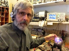
Recently I've been using the toner transfer method of board making for all but the simplest projects. I use SMT as much as possible since I don't like drilling holes. In this project I used a significant number of "leaded" components, but adapted them for surface mounting as can be seen in the photo.
The enclosure is a steel chassis I had on hand. I found that the two transformers generate a surprising amount of heat for their size and power ratings, so I'll probably drill some holes for ventilation when I put the cover plate on.
Performance and enhancements
I made a number of measurements of isolation and SWR which looked good, but here I'm speaking of on the air performance. I used the T/R switch between my Knight T-60 transmitter and Drake 2B receiver during an on the air activity for several days on 40 (mostly) and also 80 and 15 meters. No failures or problems were experienced, just smooth T/R switching.
T/R switches such as this are often integrated into a "sequencing" system which keys various transmit stages, receiver muting, sidetone and so forth. I don't have much need for sequencing at the moment but might choose to design a keyer on a PIC or AVR chip so I can simply plug my paddle into the T/R box and have outputs to key the transmitter and/or VFO. A sidetone and muting are other options I might choose to incorporate.
Do it again, smaller
I allowed myself plenty of room for this project, which in the world of boatanchors is OK. But I think I could do a lot to make it smaller, especially if the target power level were 50 W or less. First, use a single choke in each bias leg, whether molded or toroid is found to be better. Then use more SMT devices, especially for the diodes and capacitors. And surely there's something smaller than IRF830s to handle 350 mA or so in saturation and block 200 V or more with margin.
The issue of generating the "high" voltage without RF noise will still require some thinking.
A problem and a fix
I was pretty pleased using the T/R switch with "novice" transmitters like the DX-60 and HT-40, with 30 to 45 watts out. But I got a surprise when I tried it with my HT-37, which puts out perhaps 100 W.
On key down, the SWR zoomed. I eventually found that the T/R switch was switching between transmit and receive at a high rate - maybe 50,000 Hz or so. I tried many fixes and theories to no avail. At one point I found that a capacitor was "singing", but when I replaced it with a different type, it sang too. So it was responding to the problem, not causing it.
I found that I could start at low power and then run it up to 100 W with no issue, but keying at 100 W set off the oscillation.
I put it away a couple years and when I returned I started thinking about time constants. In NA6O's circuit, he used 0.022 uF capacitors from the drains of the MOSFETs to ground, and even sketched in the time constant. I didn't have that value in the voltage required in SMT so I substituted 0.1 uF. Realizing that this might be the problem, I changed those caps to two 0.01 uF units at each location and tried the switch with a 100 W transmitter. Success!
Potential builders please note: I have not changed my schematic as yet, so be aware of the change described above if you build a T/R switch based on mine.
Files
Schematics get a bit fuzzy and hard to read pasted into this blog. I'm going to put a schematic image and the ExpressSCH format file of the schematic into the Dropbox folder linked below. Also the ExpressPCB file for the board and anything else that seems useful.
References
"Electronic Antenna Switching" by Wes Hayward in QEX, May 1995. Also on EMRFD CD
"Experimental Transmitter" on the website of Gary Johnson WB9JPS (now NA6O):
http://www.wb9jps.com/Gary_Johnson/TR_Switch.html
QRZ.com page of Don Huff W6JL
Also see the Magic Box T/R switching system in 4SQRP.com, by K8IQY
I note that my schematic is very close to that of NA6O with component substitutions and power supply design variations noted.
2 comments:
Hi Nick,
Useful information for a homebrewer.
Thanks for sharing.
Basanta VU2NIL
Hi Nik!Thanks!
Post a Comment